Webcam System
Northwestern EE 326, Winter 2024
View code on GitHub ↗︎- Embedded Systems
- PCB Design
- Firmware Development
- Communication Protocols
- Hardware Debugging
The problem
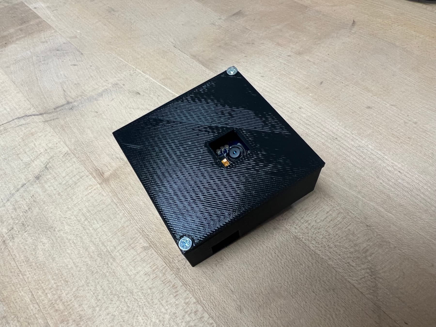
Build a webcam-style embedded system from scratch that captures images and streams them to a website. The project challenged us with end-to-end development in ten weeks: component selection, PCB design, embedded firmware, hardware bring-up, and a web interface.
System architecture
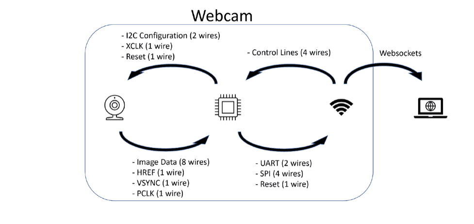
The system uses three main components:
- SAM4S8B — main microcontroller
- OV2640 — camera
- ESP32 — Wi-Fi and web connectivity
and relies on I2C, SPI, and UART communication protocols.
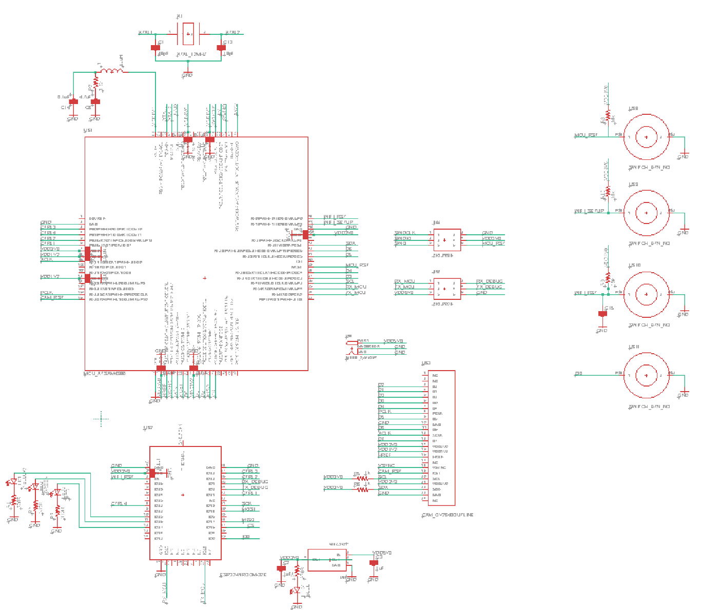
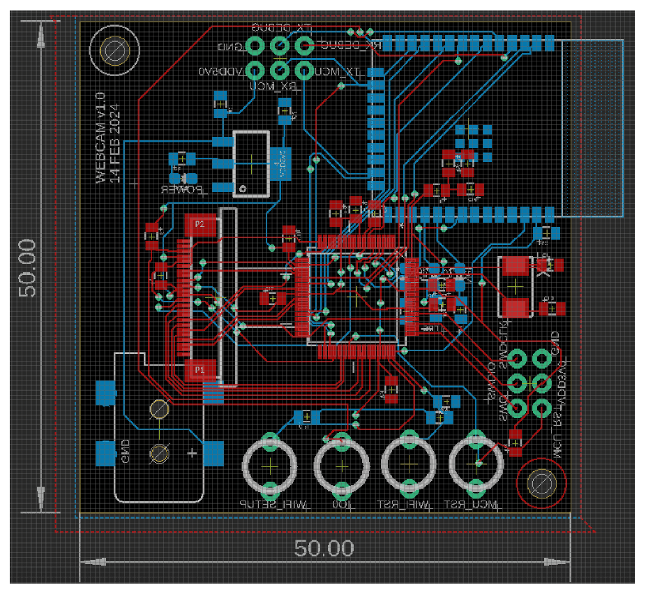
I designed a 50 × 50 mm, two-layer PCB in EAGLE.
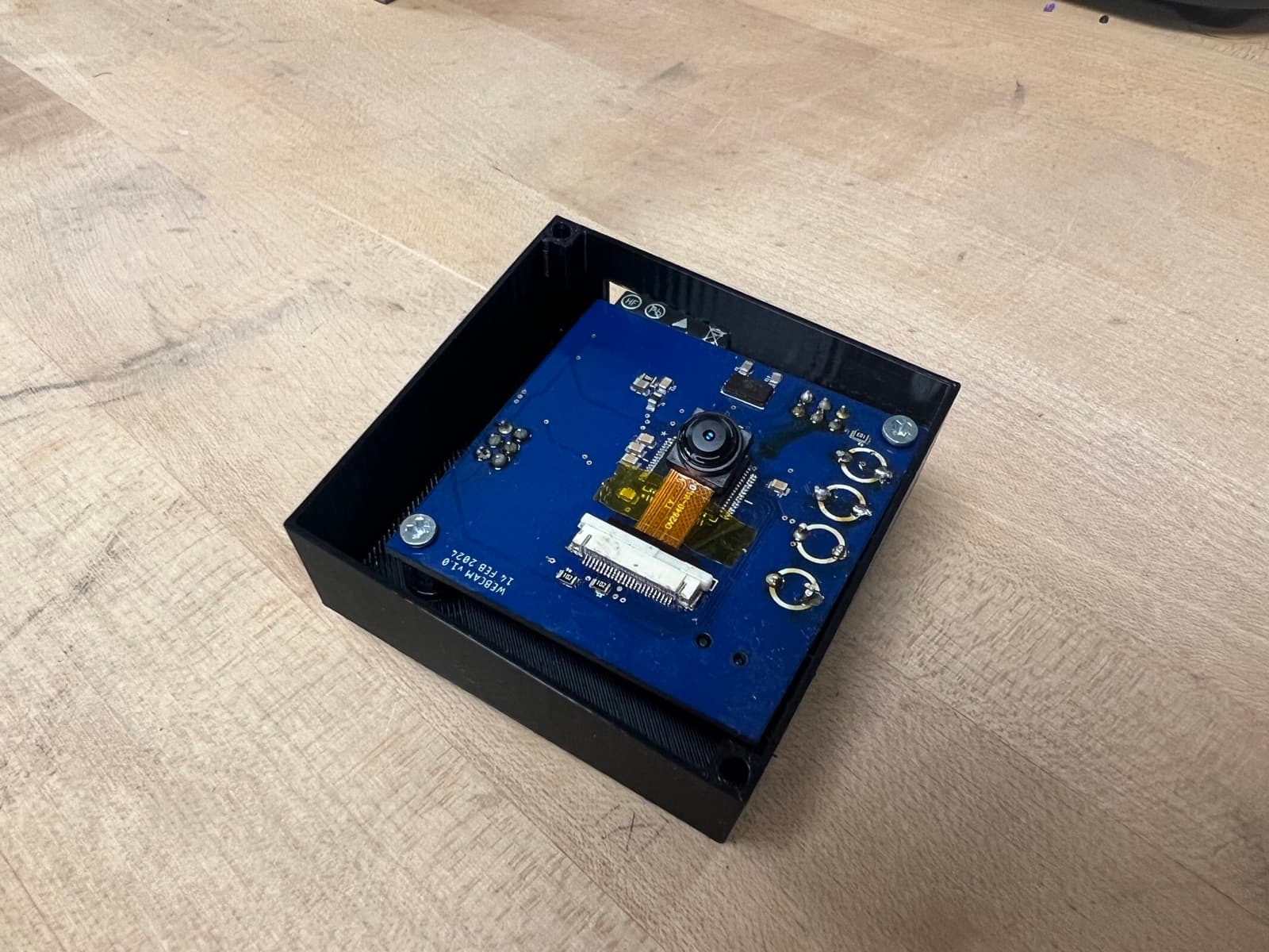
The camera and MCU sit on the outward-facing side, while the Wi-Fi module, LEDs, buttons, and barrel jack are placed on the back. This kept programming headers and reset controls away from the user-facing side.
The enclosure was modeled in Onshape and 3D printed with cutouts for the camera, antenna, LEDs, and power connector.
Firmware
The firmware was written in C using Microchip Studio and organized into separate modules for the main application, Wi-Fi communication, and camera control.
One key challenge was computing the actual JPEG length within a fixed-size raw capture buffer.
find_image_len() scanned for:
- Start of image:
0xFF 0xD8 - End of image:
0xFF 0xD9
This allowed the MCU to send only valid image data to the ESP32 over SPI rather than transferring leftover buffer data and corrupting the frame.
Debugging
The LEDs that wouldn't light: Every indicator LED on the assembled PCB stayed dark, even after changing their orientation and swapping in new parts. Serial output confirmed the board was actually entering Wi-Fi provisioning mode correctly, so the problem was specific to the LED circuit itself.
Using an oscilloscope on the LED anode and ground, I found that the expected reference voltage was jumping around rather than holding steady. The issue turned out to be in the PCB's ground plane: a ground pour had left a section of ground plane isolated from the rest of the board, so the LEDs' current-limiting resistors had no reliable return path.
Jumper wires from the LEDs to a verified ground point elsewhere restored the circuit. However, our second rework attempt to tie the isolated plane back in through nearby bypass capacitors caused a power-to-ground short. Rather than risk damaging the board close to the deadline, we stuck with the jumper wire fix and documented the issue.
The mirrored programming header: The board also could not be programmed directly through its onboard header. The schematic and net connectivity were correct, but the physical connector footprint was mirrored relative to the programmer. Jumper wires were soldered to bridged the swapped pins and allowed the remaining firmware development to continue.
The lesson learned was that issues often appear only in the physical bring-up. The experience reinforced an important embedded systems debugging principle: when firmware, schematics, and expected behavior don't agree, stop iterating blindly and isolate the problem at the physical level, e.g. analyze hardware behavior directly (scope traces, continuity, physical pinout)
Verification
I verified communication with hardware tools rather than relying only on firmware logs.
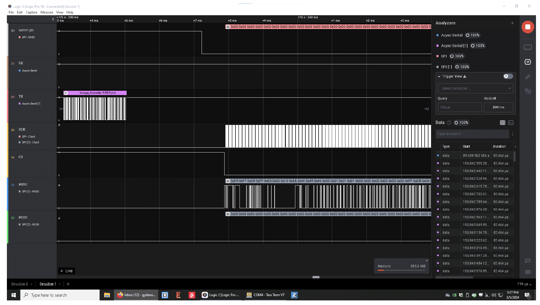
For the SPI image transfer, a logic analyzer confirmed:
0xFF 0xD8at the start of the image0xFF 0xD9at the end
This validated the JPEG boundary detection at the electrical level.
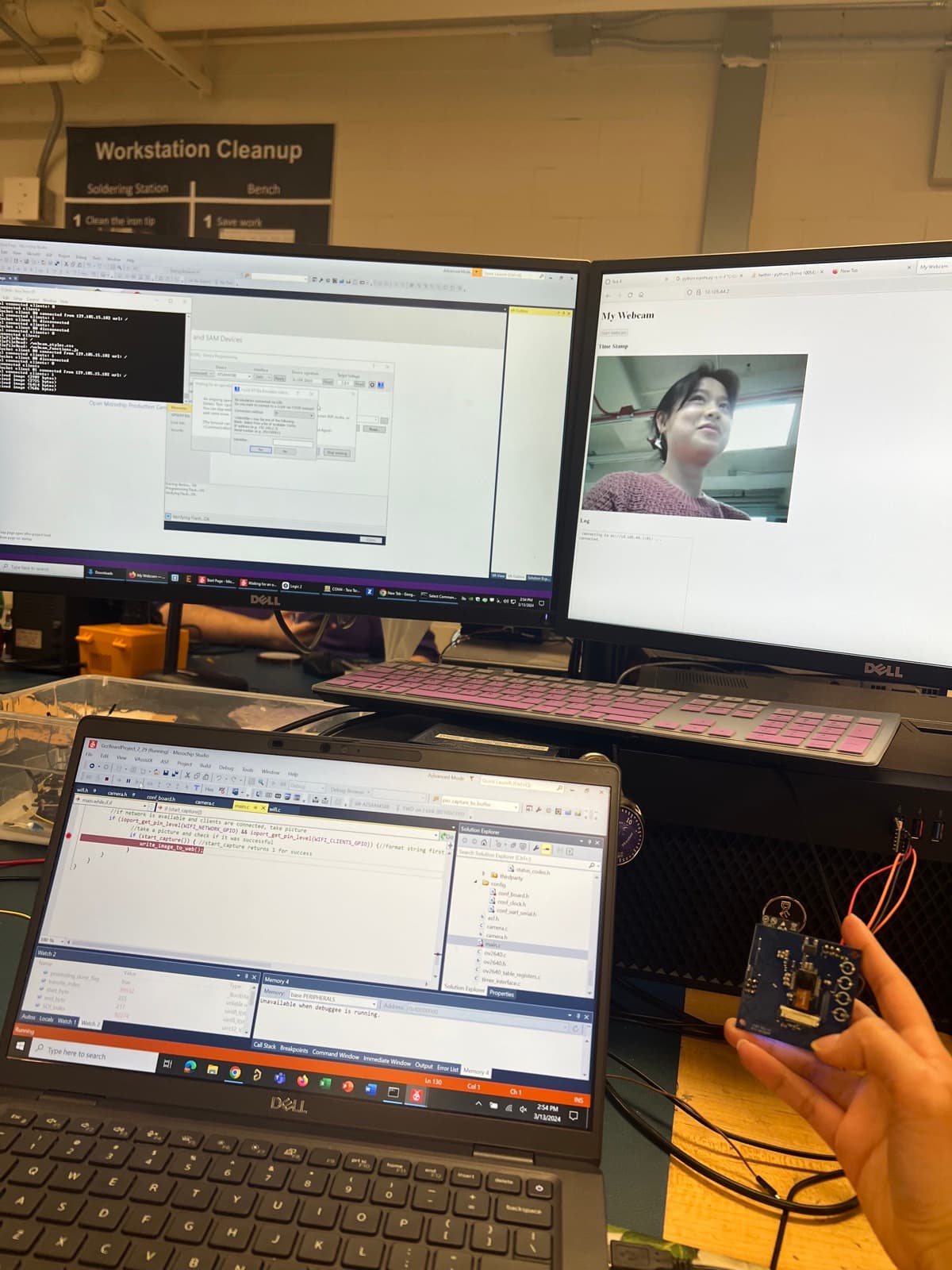
UART communication was checked with debugger breakpoints and watch windows. For example, a test command was expected to return SUCCESS.
On the web side, another issue appeared when uploaded files were silently saved as blank. The cause was traced to image file sizes, which exceeded the ESP32 file system limits. Compressing the images below 50 KB resolved the problem.
Results
The completed system captured images continuously, transferred them over SPI to the Wi-Fi module, and streamed them to a live-updating website, all while being packaged in a custom 3D-printed enclosure.
What I'd do differently
-
Review the PCB as a physical system: I would inspect ground pours and physical connector orientation more carefully before sending the board to fabrication. Both major hardware issues could have been caught with a more deliberate pre-assembly review.
-
Route strategically: Hand-routing every trace was the most time-consuming part of the build. Next time, I would manually route critical signals first (i.e power and sensitive connections) and use the autorouter where appropriate.
-
Understand interfaces before adapting examples: I would also spend more time upfront understanding the electrical behavior and configuration requirements of each communication protocol. That would reduce the amount of debugging required when adapting an existing example project to custom hardware.